A new type of lens developed in Federico Capasso's lab has gotten its first big market boost.
Jon Chase/Harvard Staff Photographer
Can tech developed at Harvard disrupt lens-making industry?
Federico Capasso believed a flat lens could revolutionize advanced products, devices. But he needed help innovating one, and getting it to market.
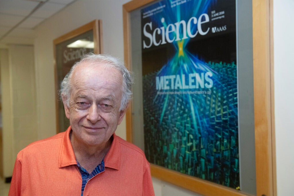
In June 2016, Alan Gordon’s phone was ringing off the hook. On the cover of the prominent journal Science was a striking image of a newly developed “metalens,” an array of tiny rectangular nanostructures that looked like skyscrapers in a vanishingly small city and focused light to a single point.
It was an invention that for years had been followed by doubt. Early results proved the concept, but the models were able to focus so little light it was thought a metalens might never be improved enough to be useful, one expert said. Later, better findings were questioned as inaccurate, and requests came in from incredulous reviewers for actual design details.
“They say it’s impossible, or you’re cheating somewhere in the system,” said Reza Khorasaninejad, a former postdoctoral fellow who was first author on several metalens papers before leaving Harvard in 2017.
But the promise for the esoteric innovation beckoned, too. Federico Capasso , the Robert L. Wallace Professor of Applied Physics in whose lab the devices were developed, had long recognized that they had the potential to do everything conventional lenses could do and more, enabling new functionality in a smaller package for all kinds of advanced devices like those for handheld facial recognition that need to “see” and do so cheaply enough that they might disrupt an industry still making lenses as they long had been, out of curved elements of glass or plastic. But it would be a long road, one that illustrates the roadblocks scientists and entrepreneurs face between the light-bulb moment and actual products.
“That’s what I liked about Federico. He doesn’t listen to these guys,” said Khorasaninejad, who worked in Capasso’s lab for three years. “He told us, ‘Let’s focus on this.’ He gave us the resources; he gave us the guidance.”
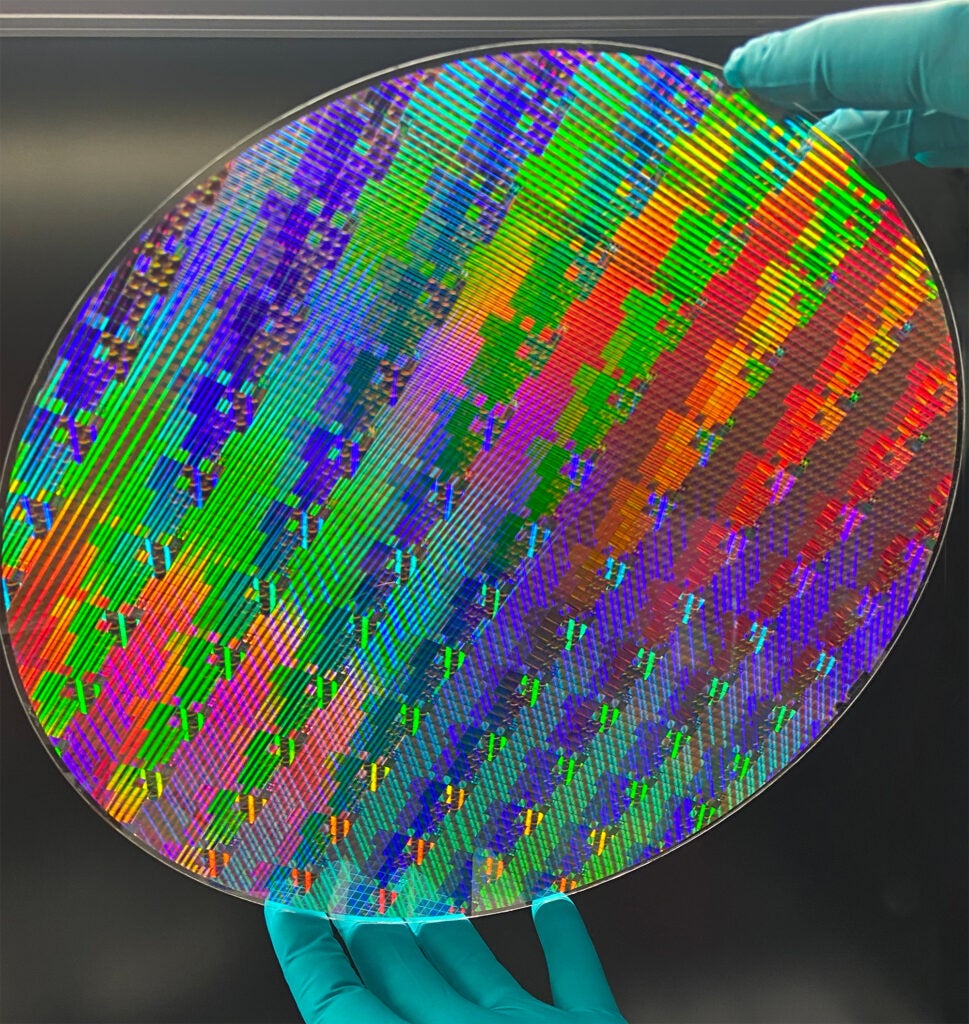
While traditional lenses use curved glass or plastic to bend light and focus an image, a metalens uses a series of tiny pillars on a millimeter-thin wafer.
Metalenz
While traditional lenses use curved glass or plastic to bend light and focus an image, a metalens uses a series of tiny pillars on a millimeter-thin wafer.
Metalenz
In early 2016, a team led by Capasso, with key contributions by Khorasaninejad, graduate student Rob Devlin, and postdoc Wei Ting Chen, showed that it indeed could be done and done well enough that commercial devices were possible. Capasso filed a report of invention with the Harvard Office of Technology Development and, soon after, the discovery made Science’s cover. Gordon , OTD’s director of business development for physical sciences, stepped in to manage the avalanche of interest.
“I’ve been doing this for far longer than I like to admit but that paper, the invention, and the patent we filed generated far more commercial interest — from companies, entrepreneurs, investors — than any other hard-tech invention I can remember,” said Gordon. “It was exciting and a bit shocking. We met and talked with a lot of people about this work.”
Those people understood then what Capasso had seen more than a decade earlier. Lenses are essential components in a host of devices, focusing and detecting light — both visible and invisible — for applications well beyond imaging, including facial recognition in smartphones and laptops, proximity and gesture detection to enhance responsive functions in automated devices, depth-sensing cameras, environmental awareness in drones and robots, and collision avoidance in self-driving cars.
In many of those devices, space is tight. The stacked elements of plastic or glass in traditional lenses have resisted the true miniaturization that most other components have undergone. They remain among the bulkier components, and a bottleneck in device design.
“I hold up my cellphone and pull out a credit card,” Gordon said, describing how he introduces the technology to potential investors. “There are only two reasons the phone is not as slim as the credit card. One is the camera and the other is the battery. The metalens will help enable the phone to be as slim as a credit card.”
While traditional lenses use curved glass or plastic to bend light and focus an image, a metalens uses a series of tiny pillars on a millimeter-thin wafer. The pillars are smaller than the wavelength of light and transparent to the desired wavelength. The pillars’ shape, the distances between them, and their arrangement on the wafer are varied to bend light as desired.
Not long after that Science cover, OTD licensed the technology to a startup, Boston-based Metalenz, founded by Capasso, Devlin, and Bart Riley, a tech entrepreneur with whom that office had previously worked. Now Metalenz’s chief executive, Devlin made a key materials advance in the Capasso lab that greatly improved the lenses’ efficiency. Earlier this year, Metalenz logged its first major sale, with manufacturer STMicroelectronics. STMicro will use metalenses in the company’s “time of flight” modules, which provide 3D sensing in an array of devices and which have previously sold 1.7 billion units. Those units appear in everything from drones to robots to smartphones. Metalenz said in June that it expects its optical components to be in millions of consumer devices this year.
Khorasaninejad, who today is CEO and cofounder of San Francisco-based Leadoptik, called the deal “a very, very strong endorsement from industry,” while Capasso said that the metalens can be made in the same factories as computer chips is potentially “game-changing,” as it unifies two industries: semiconductor manufacturing and lens-making.
“The same planar technology, known as deep ultraviolet lithography, to mass-produce integrated circuits — chips — can be used by the same foundry to make flat optics such as metalenses,” Capasso said. “It means that the entire camera module of a cellphone or laptop will eventually be manufactured in one sweep, including the metalens and the sensor.”
‘Can you get rid of the lens?’
Capasso came to Harvard in 2003 after a career at Bell Labs, where, in 1994, he and colleagues invented and developed the quantum cascade laser, currently being commercialized in devices for chemical sensing and spectroscopy.
Capasso traced the development of the metalens to a conversation he had more than a decade ago with Jim Anderson , the Philip S. Weld Professor of Atmospheric Chemistry. The two had been discussing putting a quantum cascade laser on a drone that Anderson wanted to use to detect certain chemicals in the atmosphere, but there wasn’t enough room. That was in part because of the bulky optical elements needed for focusing. Anderson got to the heart of the problem.
“He said, ‘Can you get rid of the lens?’” Capasso recalled. “My first reaction was, ‘What the hell is he talking about?’ But then I said, ‘No, wait a moment.’”
Capasso started to brainstorm the idea with a couple of students in his group. Starting in 2007 or 2008, they began to focus on the scientific question of whether it was possible to bend light in an entirely flat device.

Rob Devlin, now Metalenz CEO, made a key materials advance in Capasso's lab as a graduate student that greatly improved the lenses’ efficiency.
Metalenz
Rob Devlin, now Metalenz CEO, made a key materials advance in Capasso's lab as a graduate student that greatly improved the lenses’ efficiency.
Metalenz
Early work used what they termed “plasmonic antennas” that eventually evolved into metasurfaces — millimeter-thick, two-dimensional surfaces studded with tiny nanostructures smaller than the wavelength of light. Those arrays, Capasso said, can alter the path of light flowing through it in a kind of “artificial refraction.”
That work progressed incrementally, producing several scientific papers that led to a 2011 breakthrough, published in Science and now cited more than 5,400 times. Capasso and members of his lab demonstrated they could tune the nanostructures and bend light to a roughly focused “hotspot.”
While the results were of scientific interest, the efficiency was so low that most of the light was lost, a result that skeptics said meant it would never become useful.
Bringing fresh eyes, new skills
In 2012, Devlin joined the lab. With no optics background, Devlin instead worked in an area Capasso thought would be key: materials science and nanofabrication. Devlin himself believed that the lab had mostly figured out the science, and that choosing the right materials and fabrication processes would be critical to improved results.
“The metasurface was a great proof of concept, but the devices themselves were really inefficient,” Devlin said. “There were problems in how it was fabricated, in materials, and design.”
Devlin set about considering materials and processes that not only worked in the lab, but that would also work, if a successful device needed to be scaled up. Ultimately, he settled on titanium dioxide, a compound widely used in paint pigment, sunscreen, food coloring, and as a reflective surface in dielectric mirrors. More importantly to Devlin, it had low light-absorption properties.
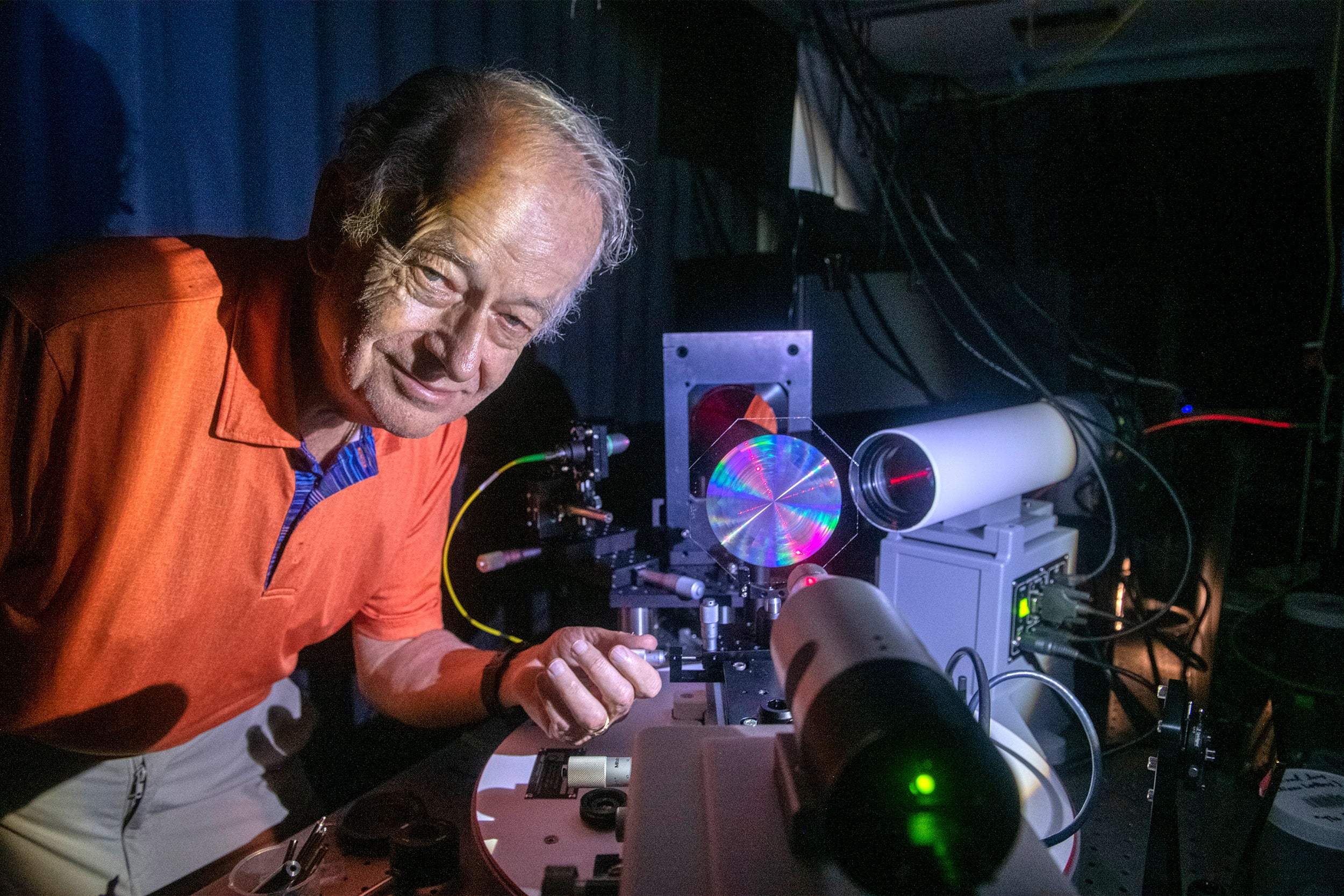
Capasso and his postdocs are working on new discoveries, including an ambitious “universal camera” that can see all properties of light at the same time.
Jon Chase/Harvard Staff Photographer
Capasso and his postdocs are working on new discoveries, including an ambitious “universal camera” that can see all properties of light at the same time.
Jon Chase/Harvard Staff Photographer
By late 2015, there were eight to 10 people in the lab working on different aspects of metasurfaces. As each turned their focus to lens performance, they brought perspectives and insights gleaned from their diverse prior efforts.
Devlin knew they had things right when the efficiency — the amount of the available light the device could focus — abruptly began to climb, rising from 10 percent to 85 percent in a few weeks. The rapid improvement and clarity of the resulting images stunned Devlin, Khorasaninejad, and Chen.
Those results spurred the 2016 Science paper, which not only generated a buzz in the lens industry, but also became a runner-up for Science’s breakthrough of the year. Despite the accolades and new belief in the promise of a metalens, it still focused just single wavelengths of light. And, while there were certainly uses for single-wavelength light — facial recognition, for example, is done by bouncing a single wavelength outside the visible spectrum off a person’s face and analyzing the light that returns — the next challenge was to produce the first “achromatic” metalens, one that focuses light across the visible spectrum.
“I locked myself in my office with Wei Ting Chen for the weekend, and I said, ‘Now we need to understand what we have done,’” Capasso said. “Our design ensured that all the colors, irrespective of where they take off, arrive at the same time in the same spot.”
It took two years, but in 2018, they became the first to report success, with high resolution.
In the meantime, though, Gordon was fielding calls from industry and advising Capasso and Devlin as to the next step of the metalenses’ commercial development. He counseled them that founding a startup around a new technology tends to be more successful than licensing it to a large corporation, where it can get lost. They listened and founded Metalenz to commercialize the invention and look for additional applications.
Devlin, meanwhile, had a decision to make. He had entered his graduate studies thinking he would pursue an academic track when he left Capasso’s lab. But he had the opportunity to be among the founders of Metalenz and shepherd the device’s development himself.
To Capasso, though, Devlin’s first priority was finishing the degree. He didn’t let up on the younger scientist, requiring he continue research and complete another scientific paper. Then Capasso ran interference with investors and companies wanting a piece of Devlin’s time.
“Federico made sure I was not abandoning the completion of my Ph.D.,” Devlin said. “He said, ‘No one is to contact Rob until he completes his dissertation.’”
Devlin defended his dissertation in 2017 and graduated in June 2018. When OTD and Metalenz announced the startup to the world in 2021, Devlin was its chief executive.
“The Ph.D. student is not always a CEO type, but some are, and Rob has shown he has the personality for it,” Gordon said.
The last several years have seen Devlin taking the company through several startup milestones, securing funds, developing relationships with manufacturers, and the recent announcement that the company’s metalenses will go into mass production.
Though Metalenz has licensed more than 20 Capasso lab patents from Harvard, Capasso and his students and postdocs are busily working on new discoveries. A current focus is on ultracompact, polarization-sensitive cameras — based on flat optics — that can detect the direction in which light vibrates after it’s transmitted or reflected, revealing otherwise invisible details of a scene. His group is involved with two collaborations with NASA on these cameras, related to Earth sciences and solar physics. He and his students are also toying with the idea of a “universal camera” that can see all properties of light at the same time, including ones that can’t be seen by existing cameras. Capasso described that challenge as “very ambitious.”
“We are here to learn, starting with me,” Capasso said. “I always tell students, ‘If you have something good, you have to give it away. Don’t keep it to yourself.’”
Share this article:
Related Articles:
Harvard: Sound transmitted by laser is ultra-high-speed Wi-Fi breakthrough
April 25, 2019 • harvard