Ebers-Moll_model_schematic_(NPN).svg

Size of this PNG preview of this SVG file:
250 × 175 pixels
.
Other resolutions:
320 × 224 pixels
|
640 × 448 pixels
|
1,024 × 717 pixels
|
1,280 × 896 pixels
|
2,560 × 1,792 pixels
.
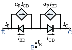
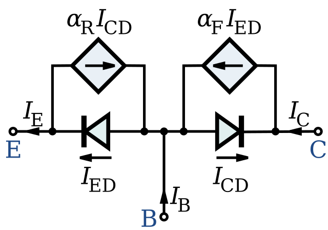
| Description | A schematic diagram of the Ebers-Moll models of an NPN BJT. The base, collector and emitter currents are I B , I C and I E , the common-base forward and reverse current gains are α F and α R , and the collector and emitter diode currents are I CD and I ED . |
| Date | (UTC) |
| Source | |
| Author |
|
This file is licensed under the
Creative Commons
Attribution-Share Alike 3.0 Unported
license.
-
You are free:
- to share – to copy, distribute and transmit the work
- to remix – to adapt the work
-
Under the following conditions:
- attribution – You must give appropriate credit, provide a link to the license, and indicate if changes were made. You may do so in any reasonable manner, but not in any way that suggests the licensor endorses you or your use.
- share alike – If you remix, transform, or build upon the material, you must distribute your contributions under the same or compatible license as the original.
Original upload log
This image is a derivative work of the following images:
-
File:Ebers-Moll_Model_NPN.PNG
licensed with Cc-by-sa-3.0-migrated-with-disclaimers, GFDL-en
- 2010-03-28T19:03:03Z CosineKitty 527x254 (13194 Bytes) Removed incorrect "+" and "-" symbols: charge carriers were backwards for NPN.
- 2010-03-28T18:44:20Z CosineKitty 527x254 (14276 Bytes) Made the following changes to fix errors in the diagram. These changes are based on the diagram on page 903 in ''Microelectronic Circuits, second edition'' by Adel S. Sedra and Kenneth C. Smith, ISBN 0-03-007328-6. 1. Revers
- 2007-09-16T00:43:26Z Kved 527x254 (10811 Bytes) {{Information |Description=NOTE: The diagram has an error. The current through the Base-to-Collector diode should be ICD, not IED. == Summary == Drawn using "Klunky" and added the minor details using MS-WORD |Source=Originall
Uploaded with derivativeFX